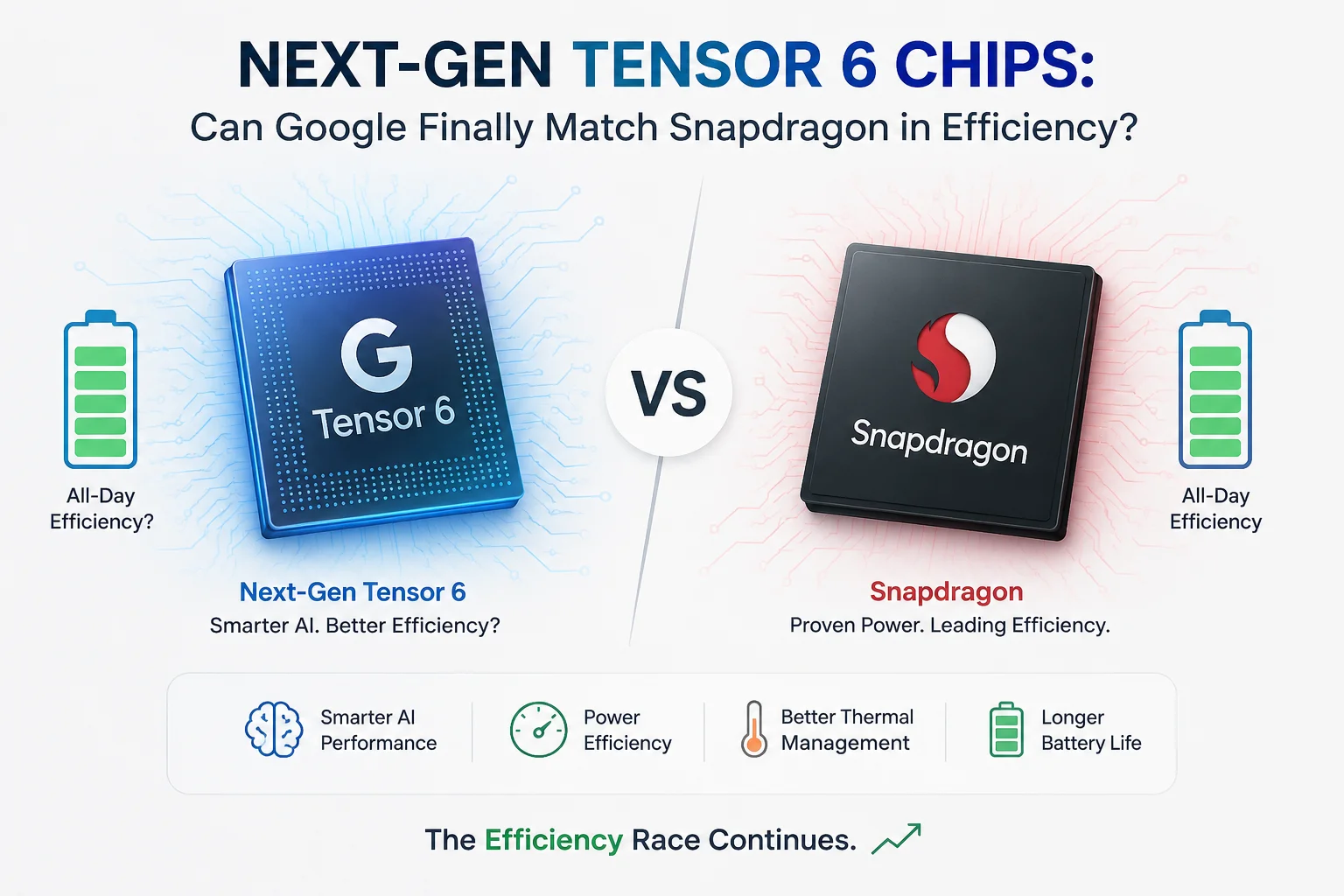
Google’s Tensor G6 arrived on August 12, 2026, powering the new Pixel 11 lineup, with expectations that it would finally close the performance gap with Apple and Qualcomm. Months before launch, leaks even suggested that Google had moved ahead of its rivals by using TSMC’s advanced 2nm process. That turned out to be wrong. Google’s VP of Hardware later confirmed that the chip is actually built on a refined 3nm process. That correction is more revealing than any specification sheet because it highlights where Google’s chip strategy is really heading.
So here's what actually happens behind the silicon: not the marketing slide, but the engineering trade-offs Google made, why they made them, and whether any of it changes how a Pixel 11 actually feels in your hand after 45 minutes of gaming or a long day of navigation and camera use.
Okay so let's talk about fast answer
Tensor G6 is built on TSMC's enhanced 3nm process (reportedly N3P), not 2nm as early rumors claimed. It brings a new 7-core CPU with Arm's C1 cores, a 50% larger TPU for on-device AI, and a reported switch to a MediaTek modem to fix Tensor's long-standing heat problem. Google claims up to 20% better power efficiency over Tensor G5. That's a real, measurable step forward — but Snapdragon 8 Elite Gen 5 already ships on the same node family with a 35% CPU efficiency claim of its own, and Qualcomm's next chip is reportedly already jumping to 2nm. Tensor G6 narrows the gap in day-to-day battery life and thermals; it does not close it on raw sustained performance.
Now What Actually Changed Inside Tensor G6
A New CPU Family, Not Just a Faster Clock
Tensor G6 drops the Cortex-X4/A725/A520 setup from Tensor G5 for a seven-core layout built entirely on Arm's newer C1 cores: one C1 Ultra prime core, four C1 Pro performance cores, and two C1 Pro efficiency cores. Google says that translates into 25% faster web browsing and 15% quicker app loading than Tensor G5. That's a meaningful jump, but notice what's missing from that sentence — there's no claim about sustained gaming performance, which is exactly where Tensor chips have historically fallen apart after ten or fifteen minutes.
The GPU Question: Still PowerVR, Still a Compromise
The GPU is where Google's priorities show up most clearly. Reports point to a PowerVR-based design with six compute units, an evolution of the GPU used in Tensor G5 rather than a clean-sheet redesign. Qualcomm's Adreno GPU inside Snapdragon 8 Elite Gen 5, by comparison, picked up a 23% performance gain, 20% better power efficiency, and 25% faster ray tracing in the same generation. If you play graphically demanding games on your Pixel, this is the part of the chip that's least likely to close the gap this year.
The Manufacturing Reality: Why "3nm" Beat "2nm"
This is the part most coverage got wrong before launch. Google's Peng Yu-chun told Taiwanese outlets directly that Tensor G6 uses an enhanced 3nm process, not 2nm — likely a cost decision, since a brand-new node is dramatically more expensive to manufacture at volume, and Google was already absorbing higher costs from the 2026 DRAM shortage that pushed the base Pixel 11 up $100 over last year's model.
What's genuinely interesting is that this doesn't actually put Google behind on paper. Snapdragon 8 Elite Gen 5 also ships on TSMC's N3P, the same refined 3nm family reportedly used for Tensor G6. Two chips, two companies, roughly the same node — which means any real efficiency gap between them comes down to core design and power management, not the manufacturing process itself. If you want the deeper mechanics of why node size doesn't automatically translate into real-world efficiency, we broke that down in 2nm vs 3nm Phone Processors: What's the Real Difference?
The forward-looking wrinkle: leaks around Qualcomm's next flagship, the Snapdragon 8 Elite Gen 6 Pro, point to a jump to TSMC's 2nm-class N2P node as early as September 2026. If that holds, Qualcomm could open up a fresh manufacturing lead within weeks of Tensor G6's launch — which says something about how brutal the pace of this race has become. Getting priority access to TSMC's newest nodes has turned into its own geopolitical story, one we covered in Can China Really Compete in the 2nm Chip Race?
Power Efficiency: Claims vs Daily Reality
Google's headline number is up to 20% better CPU power efficiency versus Tensor G5. That's a real, TSMC-confirmed generational gain. But "power efficiency" as a marketing term and "your phone lasting through a full day" are two different things, and the gap between them is usually filled by the modem, the display, and how aggressively the OS throttles under load.
| Metric | Tensor G5 | Tensor G6 | Snapdragon 8 Elite Gen 5 |
|---|---|---|---|
| Process node | TSMC N3E (3nm) | TSMC enhanced 3nm (reportedly N3P) | TSMC N3P (3nm) |
| CPU config | 1+5+2 (Cortex-X4/A725/A520) | 1+4+2 (Arm C1 Ultra/Pro) | 2+6 (Oryon Gen 3) |
| Claimed CPU efficiency gain | — | Up to 20% vs G5 | 35% vs prior gen |
| GPU efficiency gain | — | Not officially detailed | 20% vs prior gen |
| Modem | Samsung Exynos | Reportedly MediaTek M90 | Snapdragon X-series (integrated) |
| TPU / NPU compute gain | — | 50% more TPU compute | 37% faster Hexagon NPU |
Read that efficiency row carefully: Qualcomm's own claimed CPU efficiency gain is larger than Google's. The difference is that Snapdragon's number describes CPU efficiency in isolation, while Google's Tensor G6 gains are spread across a system-level redesign that includes the modem — which historically hurt Pixel battery life far more than the CPU ever did.
Sustained Performance and Thermals: Tensor's Real Weak Point
Benchmark peaks have never been Tensor's problem. The issue has always been what happens after the first two minutes, when the chip throttles hard to avoid overheating and performance drops off a cliff. Google hasn't published sustained-performance figures for Tensor G6, and that omission is worth noticing — it's usually a sign the company would rather let independent reviewers set the narrative once Pixel 11 units are in more hands after the August 20 retail launch.
The smarter read is that Google isn't trying to win a ten-minute benchmark sprint. It's optimizing for the kind of everyday load a Pixel actually sees: camera processing, background AI tasks, and Gemini Nano running locally, not console-quality gaming for half an hour straight. That's a legitimate strategy, but it also means gamers comparing raw sustained throughput should look at how Qualcomm's chips behave under identical stress tests, something we compared directly for laptop-class ARM silicon in Snapdragon X2 Elite vs Apple M-Series: ARM Gaming in 2026, where the same "peak vs sustained" gap shows up on a completely different form factor.
The Modem Switch: Fixing Tensor's Oldest Complaint
The most consequential change in Tensor G6 might not even be the CPU — it's the reported move away from Samsung's Exynos modem toward a MediaTek M90 5G modem, said to cut power draw by around 18% while supporting downloads up to 12 Gbps. Google hasn't officially named the modem supplier in its own materials, so treat this as strongly reported rather than confirmed, but it lines up with years of user complaints. Overheating during calls and weak signal handling in fringe coverage areas were consistently traced back to the modem, not the CPU or GPU, on past Pixel phones. If this reporting holds up, it could matter more for real-world battery life than anything happening in the CPU cores.
AI Acceleration: Where Google Doesn't Need to Catch Up
This is the one category where Tensor has genuinely led rather than chased. The Tensor G6's TPU gets a 50% compute increase, and paired with the newest Gemini Nano model, Google says on-device AI tasks run up to 3.5x faster while using up to 3.5x less energy per task. That efficiency-per-task number matters more than raw speed, because it directly affects battery life whenever Gemini Intelligence, Magic Capture, or Live Translate run locally instead of round-tripping to the cloud. Those gains show up directly in the camera pipeline too, which we covered in our hands-on look at Pixel 11 Pro: AI Camera or Real Photos? Is 12GB RAM Enough?
Google's Strategy vs Qualcomm's Strategy
| Approach | Google Tensor G6 | Qualcomm Snapdragon 8 Elite Gen 5 |
|---|---|---|
| Primary goal | On-device AI, camera, efficiency | Peak CPU/GPU performance |
| Node strategy | Conservative, cost-aware 3nm refinement | Aggressive 3nm-then-2nm cadence |
| GPU philosophy | Incremental PowerVR updates | Yearly Adreno redesigns for gaming/UE5 |
| Customer base | Pixel only | Dozens of OEMs (Samsung, Xiaomi, OnePlus) |
Pros and Cons of Tensor G6's Efficiency Approach
Pros
- Confirmed 20% CPU power efficiency gain over Tensor G5, on a proven, mature 3nm node
- Reported modem switch directly targets Tensor's biggest historical weakness: heat and battery drain
- Dramatically more efficient on-device AI, which reduces cloud round-trips and saves battery in real use
- Google isn't gambling on an unproven bleeding-edge node, which usually means better yields and fewer early-batch defects
Cons
- GPU remains the weakest link for sustained gaming versus Adreno
- No published sustained-performance or thermal-throttling data at launch
- Snapdragon 8 Elite Gen 5 already claims a higher CPU efficiency gain on a comparable node
- Qualcomm's next chip is rumored to leapfrog to 2nm within weeks, which could reopen the gap
Alternatives: Who Should Actually Care
If you're a Pixel loyalist
Tensor G6 is the most efficiency-conscious Tensor chip Google has shipped. Combined with the reported modem fix, it's a legitamate reason to expect better battery life than any prior Pixel generation, even without a node jump.
If sustained gaming is your priority
Wait for independent throttling tests. A Snapdragon-powered flagship, especially one running 8 Elite Gen 5, remains the safer bet for anything involving Unreal Engine 5 titles or long console-streaming sessions.
If you care about on-device AI specifically
Tensor G6's TPU gains are hard to beat right now. Google co-designs this silicon directly with DeepMind, and it shows in Gemini Nano latency and power draw.
Last Words
Tensor G6 doesn't beat Snapdragon on efficiency — it stops losing so badly. Google made real, measurable progress: a modern CPU architecture, a much stronger TPU, and (if the reporting holds) a modem swap that fixes a years-old complaint. But Qualcomm didn't stand still, and its own efficiency claims on a comparable node are still larger on paper. The honest takeaway is that Tensor G6 is Google's most efficient chip yet, not necessarily the most efficient chip on the market, and the real test will be independent sustained-performance benchmarks once Pixel 11 units ship widely after August 20.
Frequently Asked Questions
Is the Tensor G6 built on a 2nm process?
No. Despite months of pre-launch leaks, Google's VP of Hardware confirmed the Tensor G6 uses an enhanced 3nm process, not TSMC's 2nm node.
Does Tensor G6 beat Snapdragon 8 Elite Gen 5 in efficiency?
Not clearly. Google claims up to 20% better CPU efficiency over its own previous chip, while Qualcomm claims a 35% CPU efficiency gain over its prior generation. Both chips reportedly use a similar 3nm process family, so the real difference will come down to independent, real-world battery testing.
What modem does the Tensor G6 use?
Multiple reports point to a MediaTek M90 5G modem replacing the Samsung Exynos modem used in prior Tensor chips, though Google hasn't officially confirmed the supplier in its own materials.
Will Tensor G6 handle gaming better than previous Pixel chips?
Likely somewhat better, thanks to CPU gains, but the GPU is still based on an evolution of the existing PowerVR design rather than a full redesign, so it's unlikely to match Snapdragon's Adreno GPU in sustained gaming performance.
When does the Pixel 11 with Tensor G6 launch?
Pre-orders opened August 12, 2026, with retail availability across the Pixel 11, Pixel 11 Pro, Pixel 11 Pro XL, and Pixel 11 Pro Fold starting August 20, 2026.


Comments 0
Be the first to comment!