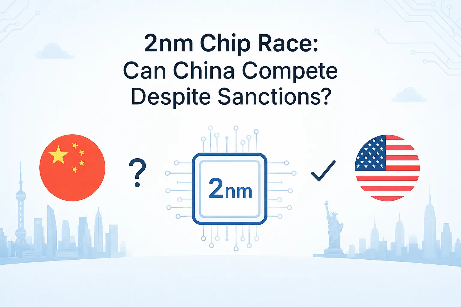
At first the quick answer is: No, not yet. China cannot mass-produce true 2nm-class chips today, and most industry estimates put a working domestic EUV lithography machine somewhere around 2032–2035. What China can do is squeeze 7nm and limited 5nm-class performance out of older DUV tools through expensive multi-patterning tricks — enough to keep Huawei's phones running, but not enough to catch TSMC, Samsung, or Intel at the bleeding edge.
So Why "2nm" Suddenly Became a Geopolitical Headline
A few years ago, chip node names were mostly a marketing exercise for engineers and gadget reviewers. In 2026, "2nm" is something finance ministers, defense planners, and AI lab CEOs argue about. TSMC's N2 process officially entered volume production in the fourth quarter of 2025, and by mid-2026 the company was reportedly pushing monthly output toward 140,000 wafers to keep up with orders from Apple, Nvidia, AMD, and Qualcomm — most of them chasing AI compute, not just faster phones.
That demand shift matters. For the first time, the majority of buyers lining up for TSMC's most advanced node aren't smartphone makers — they're high-performance computing and AI customers. Whoever controls 2nm manufacturing effectively controls the physical layer underneath the entire AI boom. That's the real reason this race gets covered like a geopolitical event instead of a tech spec sheet, and it's the same underlying tension we broke down in our look at how chip export bans are quietly reshaping global power.
What "2nm" Actually Means (Hint: It's Not Literally 2 Nanometers)
Node names haven't described a physical transistor measurement for over a decade. "2nm" is a marketing label for a generation of manufacturing that uses Gate-All-Around (GAA) nanosheet transistors instead of the older FinFET design. GAA wraps the gate completely around the channel, which gives engineers tighter control over current leakage — a real problem once transistors get packed this densely. TSMC's own technical documentation describes N2 as delivering roughly 10–15% better performance at the same power draw, or up to 30% lower power at the same performance, compared to its previous 3nm node.
The 2026 Scoreboard: Who's Actually Shipping What
Strip away the press releases and the picture in mid-2026 looks like this:
| Company | Country / Region | Node | Status (as of mid-2026) | Lithography | Reported Yield |
|---|---|---|---|---|---|
| TSMC | Taiwan | N2 (2nm-class) | Volume production since Q4 2025, ramping toward ~140,000 wafers/month | EUV | ~70–80% |
| Samsung | South Korea / USA (Taylor, TX) | SF2 / SF2P | Mass production started 2025 (Exynos 2600); Taylor fab targeting 2027 | EUV | ~50–70%, improving |
| Intel | United States | 18A | Ramping since 2025, chasing external foundry customers | EUV | ~50–55% |
| SMIC | China | N+2 (7nm-class), experimental 5nm-class | No true 2nm; stuck refining 7nm and pushing limited 5nm output | DUV (multi-patterning, no EUV) | ~20–40% |
The gap isn't subtle. TSMC, Samsung, and Intel are all shipping EUV-based 2nm-class silicon with yields that make mass production economically sane. SMIC, China's national champion foundry, is still fighting to make 7nm profitable using tools that were never designed for this job.
Behind the Curtain: What Sanctions Actually Block
The word "sanctions" gets thrown around loosely, so it's worth being precise. The core restriction isn't on chips themselves — it's on the machine that makes advanced chips possible: the EUV lithography scanner, built exclusively by the Dutch company ASML. EUV uses 13.5-nanometer wavelength light generated by blasting molten tin droplets with a laser tens of thousands of times per second, then bouncing that light off mirrors polished to near-atomic precision (most of them made by Zeiss in Germany, which is now also under export control).
Since 2019, ASML has been barred from shipping EUV machines to China under pressure from the Dutch and U.S. governments. Later rounds of controls, tightened again through 2024 and 2025, expanded restrictions to cover semiconductor manufacturing equipment more broadly, chip design software, and — as of 2026 — closed loopholes that let Chinese-owned entities buy controlled chips through overseas subsidiaries. You can read the U.S. Congressional Research Service's official breakdown of how these controls evolved on Congress.gov, and the Reuters-sourced reporting on the 2026 subsidiary loophole closure via Al Jazeera.
So How Does Huawei Keep Shipping 5nm-Class Phones?
This is the part that confuses people. If China can't get EUV, how did Huawei's Kirin chips reportedly reach 5nm-class performance? The answer is a workaround called multi-patterning — specifically Self-Aligned Quadruple Patterning (SAQP). Instead of exposing a chip layer once with EUV, SMIC exposes it up to four times with older DUV immersion scanners, offsetting each pass slightly to fake the resolution EUV would deliver in one shot. It works, technically. It's also brutally expensive, slow, and yield-punishing — reports place SMIC's advanced-node yields around 20–40%, versus 70%+ for TSMC. We covered exactly how this played out in practice in our teardown of the Huawei Pura 90 Pro Max and its sanctioned 5nm chip, which is worth reading if you want the device-level view of this same story.
China's Workaround Strategy: The Honest Pros and Cons
- Pro — Strategic independence: Even a flawed domestic supply chain reduces China's exposure to future export shocks.
- Pro — State-backed capital: SMIC's expansion is heavily subsidized, letting it absorb costs that would sink a private foundry.
- Pro — Real engineering progress: Multi-patterning DUV, domestic DUV scanners from startups, and an early-stage EUV program (reportedly codenamed "Mount Everest") show this isn't standing still.
- Con — Brutal yields: 20–40% yield at advanced nodes means most wafers produced are effectively wasted silicon.
- Con — Cost per chip: Multi-patterning can roughly double or quadruple lithography steps per layer, driving costs far above EUV-based production.
- Con — No domestic EUV at scale: Western intelligence assessments generally place a production-ready Chinese EUV tool in the early 2030s, not this decade.
- Con — Talent gap: Industry estimates point to a shortfall of 200,000+ semiconductor specialists in China through 2027.
Why AI Demand Changes the Whole Equation
This race would matter less if it were only about smartphone chips. It isn't. AI training and inference workloads are now the single biggest driver of demand for leading-edge nodes, and that changes the incentives on both sides. Western foundries are racing to expand 2nm capacity specifically because Nvidia, AMD, and hyperscale cloud providers need it for next-generation accelerators. China, meanwhile, is trying to build AI compute capacity domestically precisely because it can't reliably import Nvidia's top-tier GPUs anymore. That's part of why China has leaned so heavily into software-side efficiency instead of pure silicon superiority — a strategy we examined in our piece on how Chinese open-source AI labs are competing with Silicon Valley without matching its hardware. If you can't out-manufacture the competition, you optimize around the hardware you actually have.
The Supply Chain Is Already Adjusting
Regardless of who wins the lithography race, global manufacturers aren't waiting around to find out. Companies across electronics, automotive, and industrial sectors have spent the last two years diversifying sourcing away from single-country dependency, a trend we mapped out in detail in our report on why global supply chains are quietly shifting away from China. That diversification is a hedge against exactly the kind of scenario this article describes: a world where the most advanced chips come from a small, geographically concentrated cluster of foundries.
Alternatives: Where the World Is Diversifying Beyond Taiwan
Taiwan still produces the overwhelming majority of the world's leading-edge logic chips, which is its own risk. That's pushed real investment into alternatives:
- Samsung's Taylor, Texas fab — targeting 2nm-class SF2P+ production for U.S.-based customers starting around 2027, positioned explicitly outside Taiwan's geopolitical risk zone.
- Intel's 18A and 14A roadmap — an attempt to rebuild a credible U.S.-based foundry business, backed by CHIPS Act funding and new external customer agreements.
- TSMC Arizona — additional fabs under construction as part of TSMC's own geographic hedging strategy.
- Japan's Rapidus project — a longer-shot bet aiming for 2nm production domestically by the late 2020s.
None of these fully replace Taiwan's capacity in the near term, but together they represent the West's answer to the same concentration risk that sanctions were partly designed to create for China.
Verdict: Who Should You Actually Trust for Advanced Chips Right Now?
For cutting-edge AI, HPC, and flagship consumer silicon: Western and allied foundries — TSMC, Samsung, Intel — remain the clear choice in 2026. Higher yields, EUV-based precision, and mature supply chains make their output more reliable and cost-effective per usable chip.
For domestic Chinese demand, mid-tier devices, and strategic independence: SMIC and Huawei's ecosystem are a credible, improving alternative — just not a competitive one at the bleeding edge yet. Their real achievement is resilience, not parity.
The honest long-term read: China is not losing this race by standing still — it's losing it slowly, while getting less slow every year. Whether that trend closes the gap or just narrows it depends almost entirely on whether China's domestic EUV program clears the mirror-precision and light-source hurdles that took ASML nearly two decades to solve.
Frequently Asked Questions
Can China produce 2nm chips today?
No. China's most advanced foundry, SMIC, is currently limited to 7nm-class production (its N+2 process) with early, low-yield attempts at 5nm-class chips. There is no domestic Chinese 2nm-equivalent production at commercial scale as of mid-2026.
Why can't China just build its own EUV machine?
EUV lithography depends on components at the absolute edge of precision manufacturing — atomically polished mirrors and a tin-plasma light source that took ASML and its supply partners well over a decade to perfect. China's domestic EUV effort, reportedly nicknamed "Mount Everest," is real but still early-stage, with most outside estimates placing a production-capable tool in the early-to-mid 2030s.
Does Huawei's 5nm-class chip prove the sanctions failed?
Partially. It proves China can engineer around restrictions using existing DUV tools and aggressive multi-patterning — a genuine achievement. It doesn't prove parity: yields are far lower, costs are far higher, and the approach doesn't scale cleanly to smaller nodes the way EUV does.
Will TSMC, Samsung, and Intel keep their lead?
Most analysts expect yes, at least through the next several years, as all three push toward 1.4nm-class nodes while China is still working to stabilize 5nm-class output.
Should a business choose Chinese-made chips for advanced products?
For performance-critical AI or HPC applications, Western and allied foundries remain the safer bet today. Chinese-made chips are increasingly viable for lower-performance, cost-sensitive, or supply-chain-resilience use cases, but not yet for bleeding-edge workloads.
What would actually change this balance?
A working, production-scale domestic EUV tool would be the single biggest turning point. Short of that, incremental DUV improvements and state subsidies can narrow the gap but are unlikely to close it entirely.
Sources: TSMC N2 Technology, ASML — How Lithography Works, TechInsights — China's SMIC Plays the 7nm Card, U.S. Congressional Research Service, Al Jazeera / Reuters.


Comments 0
Be the first to comment!