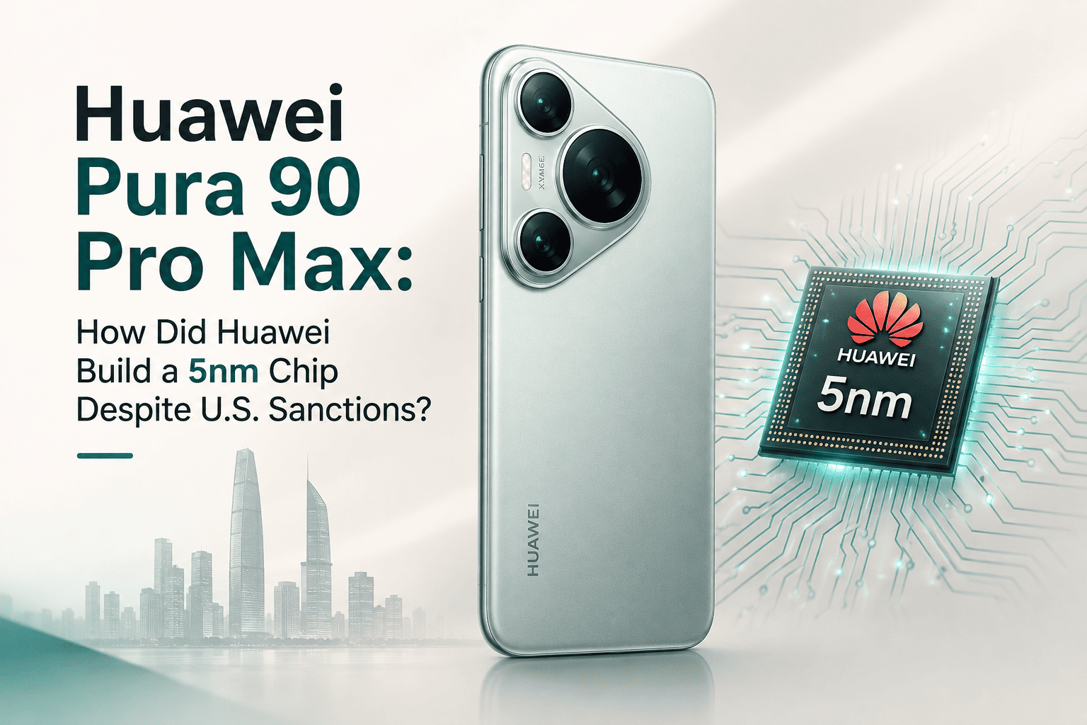
Somewhere in a fab outside Shanghai, a silicon wafer passes through the same deep ultraviolet scanner it would have used a decade ago — except this time it goes through four times instead of once, tracing the same pattern layer after layer until the lines get thin enough to matter. That's not a loophole or a smuggled machine. That's the actual, unglamorous answer to how a 5nm-class chip ended up inside the Huawei Pura 90 Pro Max, years after Washington tried to make that outcome nearly impossible.
No stolen EUV machine showed up in a shipping container. No single breakthrough moment happened. What happened instead is slower and more interesting: years of stockpiling, a homegrown design toolchain, a manufacturing trick called multi-patterning, and a domestic supply chain built brick by brick under sanctions pressure. If you've read our breakdown of how chip export bans actually work behind the scenes, this is the other half of that story — what happens when the country on the receiving end of those bans decides it isn't going to wait around.
The Pura 90 Pro Max runs on Huawei's Kirin 9030S, a 5nm-class chip fabricated by SMIC using its N+3 process — built entirely with older deep ultraviolet (DUV) lithography instead of the extreme ultraviolet (EUV) machines that ASML is barred from selling to China. Huawei got there through a mix of pre-ban EDA software licenses, a new generation of domestic chip-design tools, an aggressive patterning technique called SAQP, and a supply chain that increasingly leans on Chinese memory and packaging partners. It's a real technical acheivement, but it's also expensive, yield-constrained, and still a step behind what TSMC or Samsung ship at true 5nm.
What's Actually Inside the Pura 90 Pro Max
| Component | What It Is |
|---|---|
| Processor | Kirin 9030S, 5nm-class |
| Foundry & Node | SMIC N+3 (a scaled version of the same N+2 lineage used for the Kirin 9000S) |
| Lithography | Deep ultraviolet (DUV) with multi-patterning — no EUV involved |
| Performance claim | Roughly 25% faster than the Pura 80's chip, according to Huawei |
| Memory | Mix of Samsung LPDDR5X and, in some variants, domestic CXMT memory |
| Software | HarmonyOS domestically, Android-based AOSP build for global units without Google services |
The Sanctions Wall Huawei Had to Climb
To understand why a 5nm-class chip is such a big deal, you have to remember how thoroughly Huawei got cut off in the first place.
2019: The Entity List Freeze
In May 2019, the U.S. Bureau of Industry and Security added Huawei and dozens of its affiliates to the Entity List, requiring any US supplier to get a special license before selling it anything covered by American export rules. That single decision reached far beyond obvious hardware — it touched software, chip design tools, and manufacturing equipment made anywhere in the world using US technology.
2020: The TSMC Cutoff That Actually Hurt
The real gut-punch came in September 2020, when TSMC — the world's most advanced contract chipmaker — stopped producing Kirin chips for Huawei entirely, per updated BIS restrictions covering foreign-made products built with US tools. Huawei's last batch of TSMC-made 5nm Kirin 9000 chips became a finite stockpile with a countdown clock. According to the Congressional Research Service, this was one part of a much wider campaign involving criminal charges, entity listings, and restrictions layered on top of each other through 2020 and beyond.
By late 2020, Huawei had no legal path to the world's best chip factories. It had two choices: exit the high-end smartphone market, or rebuild the entire chip supply chain at home. It chose the second one, and the Pura 90 Pro Max is the current result of that bet.
Behind the Scenes: How SMIC Reached a 5nm-Class Node Without EUV
Here's the part most headlines skip past: SMIC doesn't have EUV machines, full stop. ASML has not shipped them to China since 2019, and that hasn't changed. So how did a 5nm-class chip happen anyway?
DUV Multi-Patterning, Explained Simply
EUV lithography can etch extremely fine circuit patterns in a single pass because its light wavelength is short enough to draw thin lines directly. DUV light is longer, so it can't naturally draw lines that fine in one shot. The workaround is to run the wafer through the DUV scanner multiple times, offsetting the pattern slightly each pass, until the combined result looks as fine as what EUV would produce in one go. SMIC's version of this is called Self-Aligned Quadruple Patterning, or SAQP — four passes instead of one.
Analysis from TechPowerUp confirmed that SMIC's N+3 node, the process behind the Kirin 9030 family, is officially China's most advanced node produced entirely without EUV tools — a full generation ahead of the N+2 process used in the earlier Kirin 9000S.
The Yield and Cost Problem Nobody Puts on the Spec Sheet
Multi-patterning isn't free. Every extra pass adds a chance for misalignment, and in the back-end metal layers where the finest wires live, that risk compounds fast. A teardown analysis reported by Tom's Hardware flagged this directly — unlike a normal node transition, N+3 gains its density through aggressive DUV-driven back-end tricks rather than a clean process shrink, and yield can fall off a cliff once the patterning budget gets pushed too far. That's a big part of why Huawei's flagship phones have a long history of shortages and slow restocks; SMIC simply can't stamp out N+3 wafers as fast, or as cheaply, as TSMC stamps out real 5nm.
Design, Packaging, and Memory: The Other Half of the Story
A chip isn't just a manufacturing process. Someone has to design it, someone has to package it, and it needs memory sitting next to it. Huawei had to rebuild all three legs of that stool at once.
Homegrown EDA Tools Filled the Gap
Chip design software, known as EDA, is dominated by three mostly-American companies. Huawei got through its earliest post-ban chips partly on a stockpile of ten-year EDA licenses bought before the 2019 cutoff, and partly by leaning on China's own EDA sector, led by companies like Empyrean Technology, which has grown rapidly since being pushed into the spotlight by sanctions.
LogicFolding: Squeezing More Density Without a Smaller Node
Because SMIC can't easily shrink further without EUV, Huawei's engineers, working with Peking University, took a different route entirely — improving density through chip design itself rather than through the manufacturing process. This approach, called LogicFolding, reportedly delivers a 53.5% jump in transistor density on the same node, and according to TrendForce, it's expected to debut commercially in the upcoming Kirin 2026 chip. It's a clever bit of engineering: if you can't get a smaller ruler, you get better at packing more onto the one you already have.
Advanced Packaging and Domestic Memory Chips
The memory sitting next to the processor matters just as much as the processor itself, and this is where Huawei's supply chain diversification really shows. Some Pura 90 Pro Max units still use Samsung memory, but others now ship with memory from CXMT, China's leading domestic DRAM maker. It's the same pattern we covered in our look at how global supply chains are quietly shifting and hedging away from single points of failure — except here it's China doing the hedging, building a second domestic source so one country's export rule can't stall an entire product line again.
Pros and Cons of Huawei's Sanctions Workaround
| Pros | Cons |
|---|---|
| Proved a 5nm-class node is possible without EUV, at least at limited volume | Yields and output remain a fraction of what TSMC or Samsung can produce |
| Reduced Huawei's exposure to any single foreign supplier | Manufacturing cost per chip is significantly higher than true EUV-based 5nm |
| Accelerated China's domestic EDA, memory, and packaging ecosystem | Still one to two full generations behind the industry's actual cutting edge |
| Gives Huawei a supply chain sanctions can't instantly switch off | Heavily subsidized — not yet proven as a commercially sustainable model |
Verdict Box: Did Huawei Actually "Beat" the Sanctions?
Short answer: not exactly, but they didn't fully work either. Huawei didn't find a way around export controls — it built its way underneath them, using older tools pushed harder than anyone expected. The Kirin 9030S is a genuinely impressive engineering feat, and it proves DUV multi-patterning can go further than most analysts assumed back in 2019. But it's also slower to produce, costlier per unit, and still trailing the actual frontier that TSMC and Samsung occupy with EUV. Sanctions didn't stop Huawei's chips from existing — they just made every single one of them more expensive and harder to make at scale.
Alternatives: What Other Paths Could China's Chip Industry Take?
- Keep pushing DUV multi-patterning further. SMIC could chase even smaller effective geometries with more patterning passes, accepting worse yields and higher costs in exchange for staying at the edge of what DUV can physically do.
- Wait for a domestic EUV machine. Chinese equipment makers are reportedly working on their own EUV tools, though most industry estimates put a usable version years away, not months.
- Lean harder into design-side tricks like LogicFolding. Instead of racing for smaller nodes, keep squeezing more performance out of nodes SMIC can already produce reliably.
- Deepen the domestic ecosystem instead of the node. Prioritize CXMT memory, Chinese EDA tools, and local packaging over chasing raw transistor density, betting that supply security matters more than being one generation ahead.
What This Means for the Global Chip Race
The bigger story here isn't really about one smartphone. It's what a 5nm-class Kirin chip signals about the limits of export controls as a tool. Restrictions were designed to slow China down by cutting off a handful of chokepoints — EUV machines, US-based EDA software, TSMC's fabs. Those chokepoints still hold at the very top of the industry. But underneath that ceiling, they pushed China to build a parallel, if less efficient, version of the entire chip stack, from design tools to memory to packaging.
That has ripple effects well beyond phones. It's the same dynamic we've tracked in our coverage of global tech and trade shifts — export rules reroute supply chains, and those reroutes eventually show up in prices and availability for ordinary buyers, whether that's a smartphone chip or the graphics card inside your next gaming rig, a trend we've also seen play out around console and PC hardware pricing. If you're tracking hardware trends generally, it's worth keeping an eye on our tech coverage as this story keeps evolving through 2026.
Frequently Asked Questions
Does the Huawei Pura 90 Pro Max actually use a true 5nm chip?
It uses a "5nm-class" chip — SMIC's N+3 node produces transistor density comparable to early 5nm processes from TSMC or Samsung, but it's built with older DUV lithography rather than EUV, so it isn't identical in cost, efficiency, or yield to a genuine EUV-based 5nm chip.
Did Huawei break US sanctions to get this chip made?
Not in a legal sense that's been proven. SMIC used equipment and techniques not directly banned for this specific process, relying on DUV tools it already had rather than smuggled EUV machines. The sanctions weren't broken so much as engineered around.
Why can't SMIC just buy EUV machines from ASML?
The Dutch government has not licensed EUV exports to China since 2019, largely due to pressure coordinated with the US. Without a license, ASML legally cannot sell or service EUV systems for Chinese customers.
Is the Kirin 9030S as good as an iPhone or Snapdragon chip?
It's competitive with recent upper-mid-tier chips in daily use, and Huawei's camera and AI processing are genuinely strong. But in raw benchmark performance and efficiency, it still trails the newest Apple and Qualcomm flagship silicon, which are built on true EUV-based nodes.
Why does Huawei's chip supply still run short sometimes?
SMIC's N+3 process is harder to produce at scale than a mature EUV node — more patterning passes means lower yields and slower output, which has repeatedly caused restock delays for Huawei's flagship phones.
What happens if the US tightens restrictions on SMIC further?
Proposed measures like the MATCH Act would target even the DUV tools SMIC currently relies on. If that happens, Huawei's chip supply becomes more dependent on whatever domestic equipment China can build, which is still less mature than DUV.
Last Words
The Pura 90 Pro Max isn't proof that sanctions failed, and it isn't proof that Huawei found some secret backdoor either. It's proof that a determined, well-funded industrial effort can climb most of the way up a wall it was never supposed to get over — slower, at higher cost, and with real limits still visible near the top. For anyone watching the broader US-China tech relationship, that's arguably the more useful takeaway than any single benchmark score: export controls buy time and raise costs, but they don't seem to buy a permanent ceiling.
Sources: U.S. Bureau of Industry and Security, Congressional Research Service via Congress.gov, Tom's Hardware, TechPowerUp, TrendForce, and GSMArena.

Comments 0
Be the first to comment!